Embedded programming
Reading AVR DATASHEET
At this moment I realize that reading was not enought for me, I have to white things in order to memorize and try to undestand how it works, You will say that it's not the goal but it's the only way for me to undestand AVR. So the following part is like a big summary of the 280 pages.PIN configurations
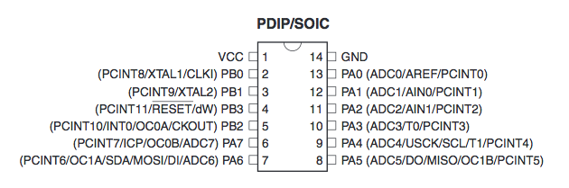
VCC : Supply Voltage.
GND : Ground.
Port B (PB3:PB0) 4-bit bi-directional I/O port with internal pull-up resistors.
RESET (PB3 when RSTDISBL fuse = 1) low level (with longer > minimun pulse length) will generate Reset.
Port A (PA7:PA0) 8-bit bi-directional I/O port with internal pull-up resistors.
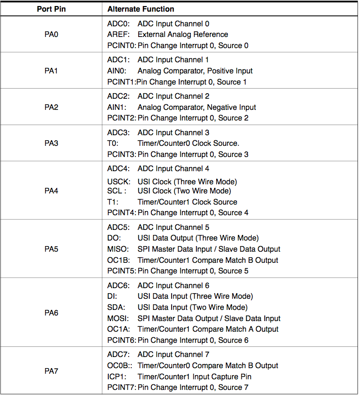
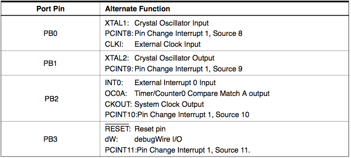
Most port pins have alternate functions in addition to being general digital I/Os:
Alternate Functions of Port A:
Alternate Functions of Port B:
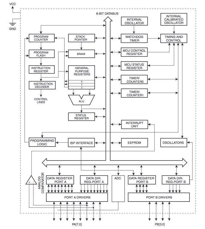
Block Diagram
Processor registers
There are 32 general-purpose 8-bit registers, R0–R31. All arithmetic and logic operations operate on those registers; only load and store instructions access RAM.
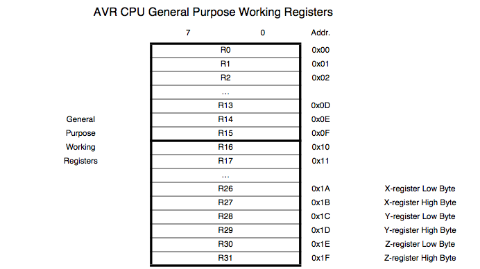
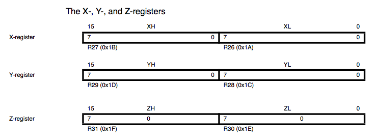
A limited number of instructions operate on 16-bit register pairs. The lower-numbered register of the pair holds the least significant bits and must be even-numbered. The last three register pairs are used as pointer registers for memory addressing. They are known as X (R27:R26), Y (R29:R28) and Z (R31:R30). Postincrement and predecrement addressing modes are supported on all three. Y and Z also support a six-bit positive displacement.
Instructions which allow an immediate value are limited to registers R16–R31 (8-bit operations) or to register pairs R25:R24–R31:R30 (16-bit operations ADIW and SBIW). Some variants of the MUL operation are limited to eight registers, R16 through R23.
In addition to these 32 general-purpose registers, the CPU has a few special-purpose registers:
PC: 16- or 22-bit program counter
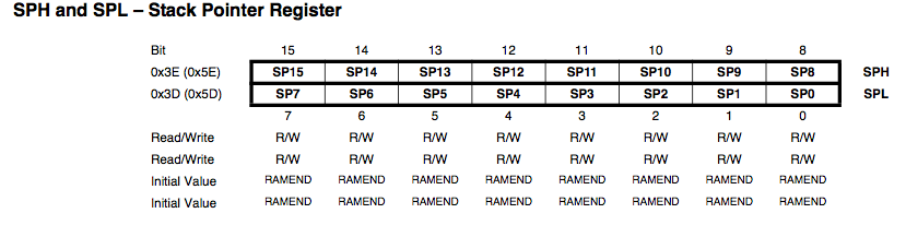
SP: 8- or 16-bit stack pointer
SREG: 8-bit status register
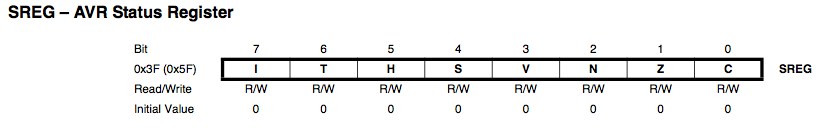
The status register bits are:
C Carry flag. This is a borrow flag on subtracts.
Z Zero flag. Set to 1 when an arithmetic result is zero.
N Negative flag. Set to a copy of the most significant bit of an arithmetic result.
V Overflow flag. Set in case of two's complement overflow.
S Sign flag. an exclusive OR between N flag and V flag
H Half carry. This is an internal carry from additions and is used to support BCD arithmetic.
T Bit copy. Special bit load and bit store instructions use this bit.
I Interrupt flag. Set when interrupts are enabled.
Memories
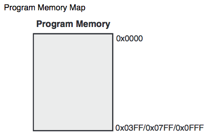
Program Memory Map
The ATtiny24A/44A/84A contains 2K/4K/8K byte On-chip In-System Reprogrammable Flash memory for program storage. Since all AVR instructions are 16 or 32 bits wide, the Flash is organized as 1024/2048/4096 x 16.
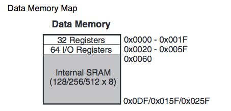
Data Memory Map
The lower data memory locations address both the Register File, the I/O memory and the internal data SRAM. The first 32 locations address the Register File, the next 64 locations thestandard I/O memory, and the last 128/256/512 locations address the internal data SRAM.
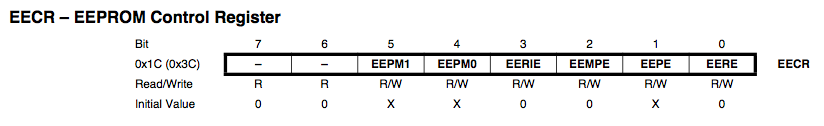
EEPROM Data Memory
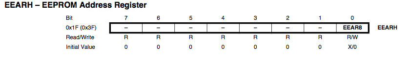
The ATtiny24A/44A/84A contains 128/256/512 bytes of data EEPROM memory. It is organized as a separate data space, in which single bytes can be read and written. it exists different procedure to write on EEPROM:
basically the user must write the address into the EEDR register:

Then the user must write the data in the EEDR register:
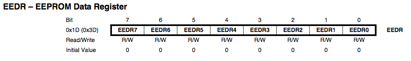
If the EEPMn bits are zero, writing EEPE (within four cycles after EEMPE is written) will trigger the erase/write operation.
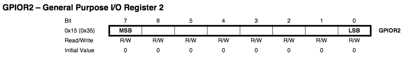
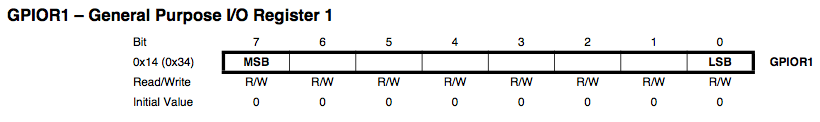
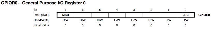
General Purpose I/O Registers
The ATtiny24A/44A/84A contains three General Purpose I/O Registers. These registers can be used for storing any information, and they are particularly useful for storing global variables andstatus flags. General Purpose I/O Registers within the address range 0x00 - 0x1F are directly bit-accessible using the SBI, CBI, SBIS, and SBIC instructions.
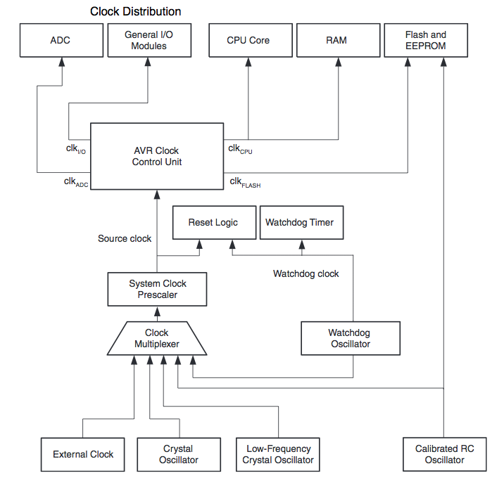
Clock System
The foolowing Picture represents the principal clock systems in the AVR and their distribution
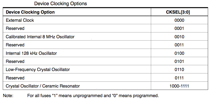
Clock Sources
The AVR has differents clock source options set by the Flash Fuse bits CKSEL[3:0]:
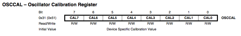
Clock Register
OSCAL: The Oscillator Calibration Register is used to trim the Calibrated Internal RC Oscillator to remove process variations from the oscillator frequency:
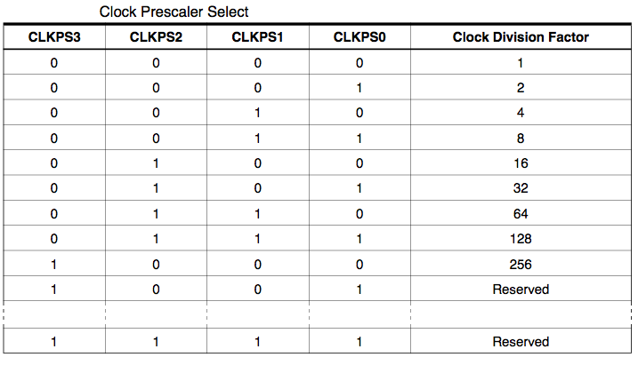
CLKPR: The Oscillator Calibration Register is used to trim the Calibrated Internal RC Oscillator to remove process variations from the oscillator frequency:
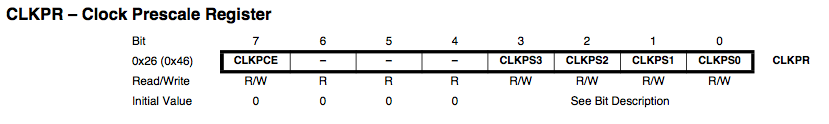
The CLKPCE bit must be written to logic one to enable change of the CLKPS bits. CLKPS[3:0]: Clock Prescaler Select Bits [3-0] These bits define the division factor between the selected clock source and the internal systemclock.
to be continued...
AVR instruction SET
For this section I will not rewrite the doc: I just put the link to atmel documentation:AVR instruction Set from ATMEL website.
C language
The last time I did C program was 20 years ago, and honestly 20 years ago I chose to be a network engineer because I didn't like the idea to be in front of a screen for rest of my life.For the academy I accept to retry language prommaming as it is a small sacrifice compare to what I will learn.
So I decided to buy the Book I used in the past:
"C LANGUAGE by Brian W. KERNIGHAN and Dennis M. RITCHIE
Python
I never program in Python but as it becomes the most used language I bought a survival guide about Python 3 by Brad Dayley.ATMEL Studio:
Even if it's seems to be a nice DevEnv I will not recommand to use Atmel Studio on Windows8.1: It changes my Path setting and also change the usb driver with one not compatible with others AVRDUDE. Even under linux It failed because I am running Ubuntu under a virtual machine which use the windows resources (including USB). Until end of May I was thinking that the problem was coming from my boards (soldering or design). Then one day I tested to burn the bootloader with Jean-Michel on his Mac and It suddenly worked. So Beginning of June a friend of mine loaned me a Mac Book Pro and It was like a new start.So because I am late on many week assignment, I will focus on the easiest enviroment: The Arduino IDE.
I swear after the rush, I will reinstall my PC and test other env.
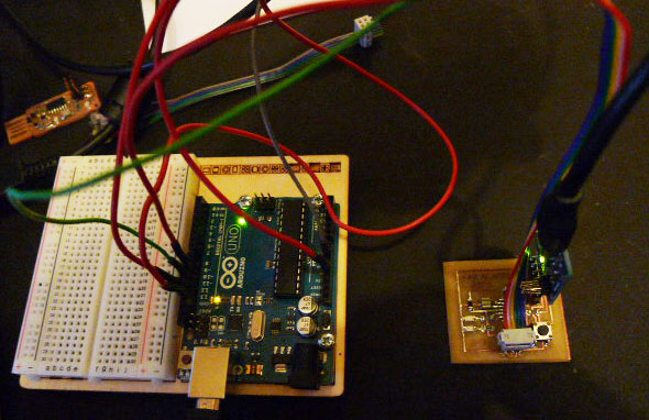
Procedure to burn bootloader and upload program Using Arduino IDE
My Pc was corrupt, a friend of mine gave my a Macbook Pro, As I don't want to install many software and envirronment on it, I will focus and use the Arduino IDE.The ISP
As I am not fully trusting my FabISP I will use An Arduino as ISP.Plug the Arduino, In File menu go to Examples and select ArduinoISP, upload the program in the Arduino.
Cabling : Slave Reset :Pin 10
MOSI :Pin 11
MISO :Pin 12
SCK :Pin 13
plug also VCC and GND the the 6 pin Connector.
Now My arduino is an ISP.
Burn the bootloader of My board
Install the Tiny board descriptor for Arduino IDE as explained in tutorial. -Plug your arduino ISP
-Plug the FTDI cable .. For extra Power
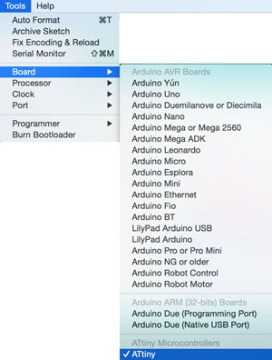
-In Tools --> Board select ATtiny.
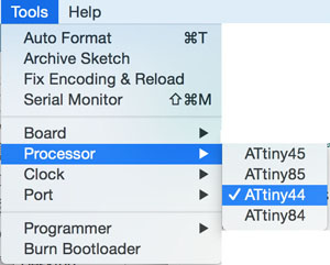
-in Tools --> Processor select Tiny44
-in Tools --> Clock Select the clock you want to use:
note: in my case it should be 20M external, but I am really not sure about the resonator and if I do the wrong choice it will be hard to go back , so because I don't need perfect clock (button and led to manage) I choose 8M internal.

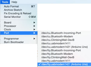
-in Tools --> Port Select the the port of the programmer, here /dev/tty.usbmodem1421 .
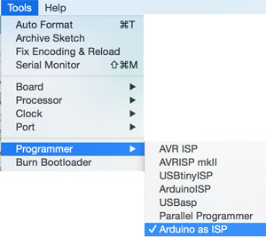
-in Tools --> Programmer Select ArduineISP .
-Then Burn the bootloader using Tools --> Burn BootLoader .
if it works you obtain the following message:
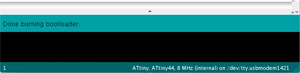
Success !!!
Upload a program :
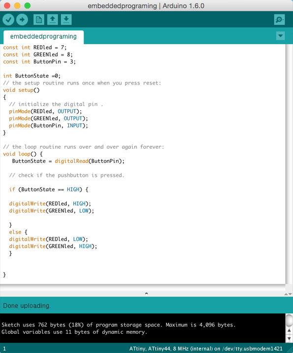
a little program which light on the red led and when you push the button light off the red led and light on the green one.
const int REDled = 7;
const int GREENled = 8;
const int ButtonPin = 3;

int ButtonState =0;
// the setup routine runs once when you press reset:
void setup()
{
  // initialize the digital pin .
  pinMode(REDled, OUTPUT);
  pinMode(GREENled, OUTPUT);
  pinMode(ButtonPin, INPUT);
}

// the loop routine runs over and over again forever:
void loop() {
   ButtonState = digitalRead(ButtonPin);

  // check if the pushbutton is pressed.

  if (ButtonState == HIGH) {

  digitalWrite(REDled, HIGH);
  digitalWrite(GREENled, LOW);

  }
  else {
  digitalWrite(REDled, LOW);
  digitalWrite(GREENled, HIGH);
  }


}
With the same setting as before and using the arduino as programmer, just click on upload.
Success !!!
Note : here the FTDI cable doesn't have the full fonctionnality (just here for power) so to upload the program I have To do it using ISP. For My Other Board JMDuino after the Bootloader burnt I just have to plug the FTDI cable and Select It As Port in Tools Port : /dev/tty.usbmodem1411.
Then when I clic on Upload it use the FTDI cable to upload the sofware.